

Call Us : 1-800-858-0604
Social Connect:


Interview with Casey Cooper, Electrical Engineering Manager, at STI Electronics Inc.
Submitted by admin on 14th of July, 2010 07:00 pm
Since 1982, STI Electronics, Inc. (STI) has been the premier full service organization for training, consulting, laboratory analysis, prototyping, and small- to medium-volume PCB assembly in the electronics industry. STI also produces a complete line of solder training kits and training support products. Additionally, the company distributes products for the electronics and industrial markets.
Q. Casey, we understand that STI’s Microelectronics Lab was established to meet the rising need for advanced systems’ development and packaging to address the emerging challenges and issues facing today’s electronics assemblies. What are some of the services offered by the lab?
A. Certified in December 2009, STI’s Microelectronics Lab is a leading edge ISO Class 6/Class 1000 Cleanroom (Microelectronics Grade) designed to produce military and medical devices that require cleanroom manufacturing standards and practices. The Microelectronics Lab provides both research and development (R&D) support to the electronics community as well as prototype, low, and mid-volume assembly services for microelectronic assemblies. Those assemblies include component packages, such as DIP and BGA packages, in addition to hybrid packages, such as MCMs, SiPs, and COB. STI’s patented packaging technology was developed in STI’s Microelectronics Lab and is supported in low-to-mid volume production today. The Microelectronics Lab also is available to provide materials and/or process qualification, including wire bond pull strength and shear testing (die shear and ball/bump shear).
Q. Can you tell us a bit about STI’s patented packaging technology— Imbedded Component/Die Technology (IC/DT®)?
A. STI has developed a patented packaging technology (Patent No. 7,116,557) coined Imbedded Component/Die Technology (IC/DT®) to integrate multiple subsystems within an electronics assembly into a single, advanced, high-density assembly. IC/DT® enables the manufacturing and assembly of high density circuit card assemblies (CCAs) to address Size, Weight, and Power (SWAP) requirements through imbedding unpackaged components in a 3-D laminate substrate with integrated thermal management. STI’s IC/DT® packaging approach addresses miniaturization, thermal management, performance, reliability, and system capability requirements through innovative design guidelines and materials selection in order to deliver reliable electronics assemblies with added functionality in the current form and fit factor.
Q. Imbedded Component/Die Technology is currently being implemented in three SBIR efforts. Can you tell us about these efforts?
A. STI is currently engaged in two parallel SBIR Phase-II efforts to demonstrate the scalability of Lockheed Martin’s SPAR-X image processor design using IC/DT® packaging technology in order to achieve a 400 percent increase in processing capability within the existing form factor. During this effort, STI has designed, assembled, and is currently testing a stacked 3-D interposer assembly using IC/DT® to imbed flip chips, bare die, and SMD components into a system card assembly for increased signal processing capabilities, improved performance, and integrated thermal management for interceptor electronics.STI also is involved in a collaborative SBIR Phase-II effort with two other small businesses to integrate multiple subsystems into a single miniaturized avionics module. The objective of this effort is to integrate the manufacturing and assembly of a digitized planar 6DOF inertial measurement unit (IMU) sensor into a single module using STI’s IC/DT® packaging technology. This integration will demonstrate higher performance in a smaller, ruggedized package for avionics applications.
Q. The increasing interest in IC/DT® created the need for a larger assembly and manufacturing laboratory, which led to the development of the Microelectronics Lab. How do customers benefit from the new lab?
A. The environment within which microelectronics are manufactured directly impacts end-product reliability. Cleanroom environmental parameters include air particulates, outgassing, temperature and humidity, and ESD. STI has met and exceeded the design requirements of ISO Class 6 (Class 1000) cleanroom requirements for particulate control and utilizes an in-house particle counter to ensure continual compliance with the ISO certification. The higher ratio of fan filter units (FFUs)-to-laboratory space enables STI to operate at or near ISO Class 5 conditions, providing a cleaner environment for manufacturing and assembly, and thus, a higher degree of reliability to the end product. Construction materials were carefully selected to minimize outgassing into the cleanroom air stream. Utilizing a high-precision building control system, STI maintains a tight tolerance on laboratory temperature and humidity conditions, thus allowing tighter process controls. STI has used multiple methods of ESD protection within the new lab, such as static dissipative flooring, static dissipative coveralls/boots, ESD grounding at all work stations, and pulsed DC ionizers directly under each FFU.
Q. The Microelectronics Lab is certified in accordance with Nebb Procedural Standards per the requirements of ISO14644-1:1999 for ISO Class 6 (Class 1000) Manufacturing Cleanroom for Electronic Hardware. Can you tell us more about the lab and who its primary customers are?
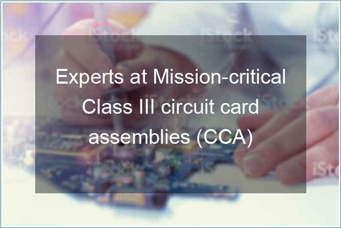
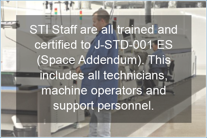
The services offered through STI’s Microelectronics Lab are applicable across all facets of the electronics industry, from commercial to medical to military and aerospace. However, those customers with stringent reliability requirements for life-critical and mission-critical products are the primary target. Electronics hardware requiring long-term warranty use in harsh environments calls for a higher-grade skill level and materials set to ensure that performance is met during operation in harsh field environments. STI’s personnel include an array of multi-disciplinary experts with decades of experience designing, manufacturing, and analyzing electronic assemblies. This experience enables STI to specialize in high-reliability hardware from design through assembly.
Q. What are some of the Microelectronic Lab’s design and modeling capabilities?
A. With experience in defense, aerospace, space, and commercial applications, STI is adept at designing and assembling electronics hardware to meet the most stringent requirements. STI uses industry-standard EDA software tools to design, model, and simulate complex system designs quickly and cost-effectively. For circuit interconnectivity, Cadence’s OrCAD Capture software is used to generate and modify schematics. From the OrCAD Capture schematic editor, a netlist and bill of material (BOM) are generated for printed circuit board (PCB) layout. STI utilizes CAD Design Software’s Electronics Packaging Designer Master PCB Designer Suite to generate the physical layout of the design. Component libraries are built per IPC-7351A standards in addition to custom component libraries for unique parts. The software package includes design rule checking (DRC), boundary creation, gerber artwork output, advanced routing/automated routing, high-speed calculations, and 3-D design output for design for manufacturability (DFM). The software also interfaces with third-party software for simulation and analysis through software from Ansoft, Mentor, and Allegro.
Q. STI is involved in research and development programs, both in component packaging technologies and electronics assembly manufacturing. What has the company done to further the development of these fields?
A. STI uses a synergistic approach to addressing those challenges faced by the electronics community. The three laboratories comprising STI’s Engineering Services division (ISO 9001:2008 certified) utilize some of the most advanced equipment for R&D, prototyping, and analysis. The owners of STI, the Raby family, continue to invest in leading-edge equipment, thus enabling engineers and analysts at STI to provide the highest quality services to manufacture an array of electronics hardware, and to address the challenges and issues facing today’s electronic manufacturers. As problems arise in the manufacturing process, the Analytical Lab provides a wide range of services designed to characterize materials, detect failure modes, and perform exploratory analysis of products or processes.
The Microelectronics Lab consists of over 1000 sq. ft. of ISO Class 6 (Class 1,000) cleanroom laboratory space for process development and assembly of hybrids and microelectronic systems, including STI’s patented packaging technology, Imbedded Component/Die Technology (IC/DT®). Through product design and manufacturability analysis, to pre-production prototype and development, STI’s Prototype and Contract Manufacturing Lab is a full service design review and pre-production facility. With two high-speed automated assembly lines, the lab supports high and low-mix PCB assembly for volumes that range from just a few units for prototypes, to low quantities for pre-production, to thousands in mid-volume production.
Q. Should we expect to see any innovations from The Microelectronics Lab during the remainder of 2010?
A. The engineering staff in the Microelectronics Lab is continually evaluating new assembly materials and processes to further improve component-level and system-level reliability. STI is currently working with several other small businesses to develop reduced form factor custom packages for use in avionics and military environments. Stay tuned!
Interview with Casey Cooper, Electrical Engineering Manager, at STI Electronics Inc.
Publication date: 15 July 2010
Newsletter


Copyright © STI Electronics, Inc. 2025. All Rights Reserved.