


Electronics Manufacturing
- Contract Assembly
- Prototype Development
- New Product Introduction (NPI) Builds
- Process Development
- Design for Manufacturing (DFM)
- Box Build & Test
- Rework & Repair
- Feasibility Assessment
- Cleanliness Testing & Validation
- Experimental Design & Processing (Electronics DOE)

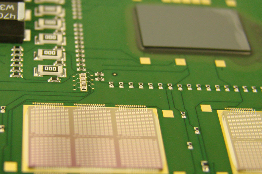
STI is equipped with a state of the art 26,000 sq ft manufacturing area with the latest in high speed placement, inspection, and test equipment in addition to work cells to assemble complex box builds. Our personnel are uniquely qualified to assemble to the highest quality standards and are all trained and certified to J-STD-001 (Space Addendum). This includes all technicians, machine operators and support personnel.
Placement capability includes surface mount high speed placement of components down to 01005 in size. Our Juki FX-3 and KE2080-L pick and place machines offer placement rates that can compete with any contract manufacturer. Inline and secondary automatic optical inspection (AOI) ensures in-process control for placement accuracy of components. STI’s reflow operation is performed in a 12-zone oven to ensure proper profile and temperature ramp (± 2°/s) to eliminate thermomechanical overstress due to wide variance in thermal exposure. This is especially critical on large, fine-pitch devices (e.g. BGAs, etc). Additionally, high speed through-hole component processing is available using our Juki selective solder machine which automates through-hole soldering for higher volume applications.
At STI, product quality is our top objective. All processes are governed by a quality system certified to AS9100 with manufacturing and inspection in accordance with IPC J-STD-001 (Space Addendum). All completed assemblies are washed and visually inspected after each process. BGA devices are 100% X-RAY inspected, and X-RAY images are available upon request. Flying probe testing is available to detect any opens and shorts on the assembly as well as to provide statistical analysis for device tolerances. Final inspection and packing is performed by IPC-certified inspectors with 10+ years in past performance experience with critical hardware. STI has 20+ years in past performance building mission-critical Class III circuit card assemblies (CCA). Documentation of past performance and references are available upon request.

STI strives to be a complete partner from schematic forward design through first article validation. A key step in this cycle is prototype development process. Prototypes are a requirement in the design validation step and often consume more funding and time than initially budgeted. STI’s unique prototype development approach mitigates these expenses and reduces the overall time to market for our customer’s new products.
The typical approach to prototype development is to design, check, build and evaluate. Upon completion of the evaluation, boards are “re spun” to implement changes desired thus adding time and money to the development cycle. STI’s approach is different with our objective focused on the implementation of corrective actions via rework and repair per IPC 7711/21 (STI is an approved development center for IPC 7711/21) to get the first prototype to the customer’s desired “production” performance level. The product can be released for beta build and test once this milestone is achieved. STI’s prototype development approach reduces the overall cost and time to market by compressing the development stages from as many as 6 cycles to as few as 2 cycles. The prototype development process is complimented by the capabilities in our analytical lab. The prototype can be subjected to environmental and analytical tests as required. These include but are not limited to thermal shock, vibration, humidity, etc. Our tests can be performed to customer-supplied specifications or a customized test plan based on best practices learned over the years. We also have the ability to test prototypes to failure to provide feedback as to the most vulnerable part of the design.
 STI’s goal for being your partner for new product introduction (NPI) is one of transparency. At STI, we see our NPI role as being a gateway to high volume production. We understand the need for data exchange throughout the entire process to guarantee a seamless transfer. We will assign a project manager who will work closely with your team to mutually develop and define requirements so as to avoid any delay caused by miscommunication. By working together transparently, STI can bridge the gap between your concept and volume production through effectively executing your NPI builds.

The best electronics assembly design won’t necessarily become the product you envision without carefully selected materials and solid manufacturing processes. STI is staffed with experienced and skilled process engineers who understand the impact of the materials selected and process parameters used to manufacture electronic hardware. In addition, design engineers at STI are available to generate special tooling and custom fixtures to ensure that your final product meets your form, fit, and function requirements.
• Assembly materials selection
• Manufacturing process parameters
• Special tooling
• Custom fixture design

STI’s engineering team places emphasis on defect prevention and non-value added process step elimination by analyzing the design data package for common errors relating to the BOM selection, PCB design, and manufacturing materials/processes used to assemble the customer’s product. In this day of global competition, STI understands that the key to a successful product is quality, cost, and speed to market. Design for manufacturing (DFM) and design for test (DFT) services offered by STI ensure quality of the final product and facilitate an efficient manufacturing cycle from fabrication, assembly, testing and ultimately through delivery. Ensuring that the customer’s design aligns with existing manufacturing processes and materials will result in higher yields and fewer design iterations to generate a product that is easily and economically manufactured.
• BOM Analysis
• Component Review
• Availability/Alternate Selection
• PWB Drawing Review
• Test Point Access
• Form/Fit Requirements
• Fabrication Note Review
• Soldermask Clearance
• Silkscreen Identifiers
• PWA Manufacturing Analysis
• Fiducials for Automated Assembly
• PWB Depanelization Requirements
• Land Pattern Review
• Component Placement for SMT
• Assembly Materials Selection
• Manufacturing Process Parameters

Circuit card assemblies (CCAs) and box builds have been STI’s expertise for many years. Our commitment to quality and customer satisfaction is what separates us from our competition. STI is proud to be ISO 9001:2008 certified which means that we consistently manufacture products that meet our customer’s requirements. We are vertically integrated and can take your product from concept to design through manufacturing, i.e. from prototype to full production. STI also offers logistics services for consignment and/or turn-key builds with components and materials from trusted suppliers. When you add our state of the art analytical lab for product reliability and assurance, you get a true one stop/one solution electronic manufacturing services (EMS) provider that is capable of meeting all your box build & test product requirements.
• PCB assembly services
• Testing services
• PCB coating and/or encapsulation
• Manufacturing and testing
• DFM/DFT analysis
• Leaded or lead-free solder assembly
• Touch screen integration
Turnkey systems
If you have decided to outsource your production of electronic assemblies and/or box builds, consider STI Electronics as your service provider. We are located in Huntsville (central north Alabama) in close proximity to the Army’s Redstone Arsenal base and NASA’s Marshall Space Flight Center. STI is a company committed to quality, service and the success of our customers.
REWORK & REPAIR
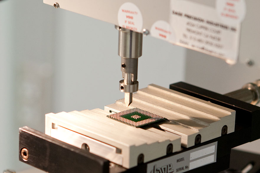
STI has qualified technicians trained in IPC 7711/7721, as well as in custom design solutions, to address your electronic rework and repair needs. Our services encompass both mainstream assembly technologies (surface mount and through-hole) as well as specialized processes that include ball grid array / BGA reballing and leadless chip carrier rework.
- BGA Rework
- BGA Reballing
- PCB Repair
- CCA Rework
- Jumper Wire / White Wire Services
Warranty BGA Repair BGA rework and repair can be a daunting task if you don’t have an experienced technician with the right tool set. At STI, we offer trained technicians utilizing top of the line BGA rework systems to complete the tasks in accordance with IPC standards. STI offers high-reliability, cost-effective reballing services to restore all of your BGAs to their original specifications. We have the capability to handle most of today’s BGA package sizes and ball counts and offer both standard reballing fixtures in addition to custom designed fixtures for a wide range of component package styles.
- Removal and replacement
- Site preparation
- Salvage
- Circuit design changes
- Pad/trace repair
- Solder mask Repair
PCB Rework & Repair – Jumper wire adds Circuit card assemblies (CCA) today are more complex and miniaturized which requires highly-skilled technicians trained to IPC certifications to successfully perform circuit board rework and repair. Our experienced technicians and engineers will diagnose and serve your repair and rework needs.
- Plated Thru-Hole
- SMT (QFP, PLCC, Chip Style, LCC, SOP)
- BPGA, CBGA, Micro BGA
- QFN and Lead less packages
Connectors Sometimes prototypes or new layout boards need to have jumper wires, i.e. white wires, added to troubleshoot and/or verify design modifications. STI stands ready to help diagnose circuit board issues and perform design layout verifications by offering jumper wire solutions. These white wires can be run underneath microBGAs, QFNs, and other leadless chip carrier style packages to troubleshoot and/or perform verification.
 Engineers at STI are available to perform a design feasibility assessment as you begin developing the standards your next product or revision upgrade. Our design engineers will provide objective feedback on key design issues such as functional requirements, form and fit factor, thermal performance, environmental resistance, reliability/warranty performance, and manufacturability. By taking these critical design points into consideration early in the design phase, STI can help reduce cost and time to market through a reduction in your product design cycle.
• Thermal Performance
• Heat sink, enclosure/housing design
• Environmental Resistance
• Temperature, humidity, vibration, shock
• Component Selection
• Functional requirements, form factor, performance
• Form and Fit Factor
• Miniaturization, interconnectivity, weight/mass
• Reliability
• Warranty expectations
• Manufacturability
• DFM, DFT, reliability
A New Method for Cleanliness Testing & Validation
When it comes to electronics cleanliness…
What you can’t see CAN hurt you.
Ionic ChromatographySIRVisual
Step 1
Cleanliness Testing
Visual Assessment
- Parts mounted on glass for visual inspection


SIR Testing
- SIR testing on component specific boards
- Reveals the impact of residues on electrical performance


ION Chromatography
- Used to identify the specific ionic species present


Step 2
Custom Test Vehicles
Custom Designed Boards
- Mimics the production boards
Custom Selected Components
- Reproduces the specific areas of concern in the process
Duplicates Process and Materials
- Provides a more representative test result

The Difference
Surface Insulation Resistance (SIR)
- We provide component specific boards for SIR testing
- Lets you correlate SIR and IC test results
on the same board using your specific
component set
Diagnostics
- What to do with all the test data?
- Use industry baselines
- Develop your own criteria
- Let us analyze the data for you
Product Acceptance
- We make it easy to go beyond the standard industry tests
Objective Evidence
- The most realistic true objective evidence

![]()
WHAT’S NEXT
Contact Us
to find out how the next generation of cleanliness
validation can provide you and your customers with
confidence in YOUR product
Mark McMeen
Vice President of Engineering Services
mmcmeen@stiusa.com • 256-705-5515
STI helps customers understand their layout parameters, processing challenges, component selections, laminate materials, and enclosure materials. These decisions, in some cases, can be quite detailed and considered a multi-variable analysis. To this end, STI provides evaluation services combined with custom design of experiments (DOE) to help guide engineers to sound design and processing choices. STI creates a custom DOE that is co-developed with the customer’s design engineers to gather the data necessary to understand those multi-variable issues. STI’s approach is to create a DOE that gathers data to develop a full understanding of the interrelationship of the variables as well as the ability to replicate the variable sets. This ensures a full understanding of the impacts of a multi-variable problem.
The DOE is a custom designed test protocol to gather and quantify the data into a format that enables a decision to be reached on the problem at hand. STI utilizes the assets of its multi-disciplined departments to develop these unique DOEs that aid in defining and understanding the complex relationship between material choices, component selections, board design layout, processing materials (i.e. flux selection, alloy composition, etc), as well as their impact on the assembly process and reliability of the final product. These variables all play a role in the product’s performance and its ability to meet the design objective and warranty expectations. Examples of variables to be considered in a customized DOE are as follows:
• Flux type and alloy composition for solder interconnects
• Cleaning requirements
• Component selection
• Layout requirements
• Laminate choice and PCB layout design
• Processing requirements
• Processing aids
• Enclosure requirements
• Harsh environment design guidelines
• Reliability and warranty expectation
Engineering
- Circuit Design
- Schematic Forward Design
- PCB Layout & Design
- System Level Integration
- Size, Weight, & Power Reduction (SWAP)
- Design for Manufacturing (DFM)
- Material Optimization
- Cleanliness Testing & Validation
- Environmental Test Services
- Electrical Test Services
- Mechanical Test Services
- Thermography Test Services
- Strain Gage Testing
 STI’s involvement in research and development programs, both in component packaging technologies and electronics assembly manufacturing, has brought about the acquisition of the top people in this field and the installation of the latest and most advanced equipment and circuit design tools. STI is US-based, ITAR registered, and staffed with engineers to design, develop, and assemble a ruggedized electronics assembly in compliance with our customer’s specifications. With experience in Defense, Aerospace, Space, and commercial applications, we are adept in circuit design and the assembly of products to satisfy our customer’s requirements.

STI offers proven experience and expertise to provide our customers with the highest quality design services. STI specializes in complex and high-reliability projects working as an extended arm to our customers’ engineering team. With today’s advanced technologies, STI understands the demand to deliver a quality design to our customer’s specifications on time and on budget.
• Analog and Digital Designs
• High Frequency RF Layouts
• Controlled Impedance Designs
• Design Attributes
• Rules Management
• Design Library Generation
• Part, Package, and Electrical Symbols
• Full Forward/Back Annotation
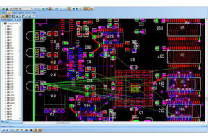
 Even the best schematic circuit design can be undermined by poor component layout and routing. STI’s experienced design engineers address the critical design factors that affect manufacturing and assembly, product performance, and long-term reliability. The PCB layout and design services offered by STI combine experienced electrical, mechanical, thermal, manufacturing, and test engineers’ knowhow to ensure that the resulting PCBs fly through assembly, test, and ultimately to field thus helping to reduce product development costs.
• RF Design
• Tuned Routing
• Shielding
• High Speed Routing
• Bypass/Filter Component Placement
• Controlled Impedance Routing
• Matched Length Rules
• Differential Pair Routing
• Forward/Backward Annotation
• Library Creation and Maintenance
• Land Pattern Optimization
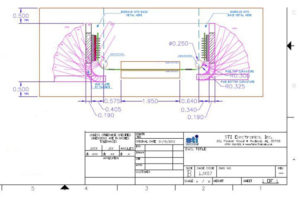
 Assembly documentation is necessary to capture all of the materials, processes, and final requirements of board-level and system-level assemblies. These drawings convey material sets, approved assembly processes, final inspection requirements, and upper-level assembly specifications. STI provides system level integration services for completing this documentation process as well as assists in identifying key assembly materials, processes, and inspection requirements.
• Wiring Diagram
• Box Build Documentation
• Full Assembly Drawings
• Workmanship Standards Referencing
• Mechanical Detail
• Dimensioning
• Tolerance Stack Up Analysis
• Material Compatibility Review
• Thermal Interface Material Selection
 Military and aerospace electronics providers continue to push the technological envelope to design and manufacture leading edge electronics for today’s users. Current design problems are not driven by circuit design capabilities but by an inability to reliably package these circuits within the space constraints. Innovative packaging techniques are required in order to meet the size, weight, and power (SWaP) reduction requirements of this industry without sacrificing reliability or performance.
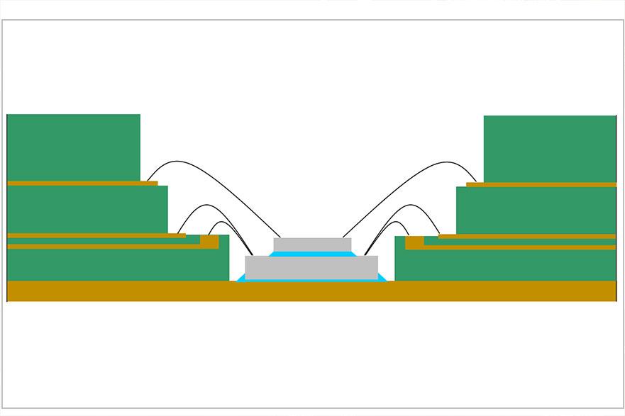
STI’s design engineers utilize conventional hybrid and microelectronics technologies to enable our customers to meet their SWaP requirements in addition to STI’s patented packaging technology termed Imbedded Component/Die Technology (IC/DT®). IC/DT® enables the manufacturing and assembly of smaller, lighter, and more technologically advanced high density circuit card assemblies where conventional packaging technologies fall short through imbedding unpackaged components in a 3-D laminate substrate with integrated thermal management. STI’s IC/DT® packaging approach addresses miniaturization, thermal management, performance, reliability, and system capability requirements through innovative design guidelines and materials selection in order to meet form, fit, and function requirements.
• Reduced Form Factor
• Miniaturized Components
• Increased Performance
• Ruggedized Applications
• Reduced Interconnects
• Space Constraints
• Imbedded and/or Stacked Components
• Low-Weight Solutions
• Light Weight Interconnects
STI’s engineering team places emphasis on defect prevention and non-value added process step elimination by analyzing the design data package for common errors relating to the BOM selection, PCB design, and manufacturing materials/processes used to assemble the customer’s product. In this day of global competition, STI understands that the key to a successful product is quality, cost, and speed to market. Design for manufacturing (DFM) and design for test (DFT) services offered by STI ensure quality of the final product and facilitate an efficient manufacturing cycle from fabrication, assembly, testing and ultimately through delivery. Ensuring that the customer’s design aligns with existing manufacturing processes and materials will result in higher yields and fewer design iterations to generate a product that is easily and economically manufactured.
• BOM Analysis
• Component Review
• Availability/Alternate Selection
• PWB Drawing Review
• Test Point Access
• Form/Fit Requirements
• Fabrication Note Review
• Soldermask Clearance
• Silkscreen Identifiers
• PWA Manufacturing Analysis
• Fiducials for Automated Assembly
• PWB Depanelization Requirements
• Land Pattern Review
• Component Placement for SMT
• Assembly Materials Selection
• Manufacturing Process Parameters
 While the bill of materials (BOM) is generated at the start of the design process, it is utilized by procurement and plays a critical role in driving price and schedule of a customer’s product. While some product’s time to market is short, other products may see months to years of testing before a manufacturing release. Therefore, a material review and optimization can eliminate costly production time due to inaccurate/changed part numbers, obsolete components, and long-lead/non-stock components. Also, it is critical to ensure that counterfeit devices are not procured through the use of authorized distributors and trusted suppliers. STI offers these services to mitigate risk and reduce cost during the BOM purchasing process.
• BOM Scrubbing
• Validate Manufacturer Part Numbers
• Procurement Resource Planning
• Component Obsolescence
• Identify Approved Alternates
• Trusted Supplier Analysis
• Validate Authorized Distributors
A New Method for Cleanliness Testing & Validation
When it comes to electronics cleanliness…
What you can’t see CAN hurt you.
Ionic ChromatographySIRVisual
Step 1
Cleanliness Testing
Visual Assessment
- Parts mounted on glass for visual inspection
SIR Testing
- SIR testing on component specific boards
- Reveals the impact of residues on electrical performance
ION Chromatography
- Used to identify the specific ionic species present
Step 2
Custom Test Vehicles
Custom Designed Boards
- Mimics the production boards
Custom Selected Components
- Reproduces the specific areas of concern in the process
Duplicates Process and Materials
- Provides a more representative test result
The Difference
Surface Insulation Resistance (SIR)
- We provide component specific boards for SIR testing
- Lets you correlate SIR and IC test results
on the same board using your specific
component set
Diagnostics
- What to do with all the test data?
- Use industry baselines
- Develop your own criteria
- Let us analyze the data for you
Product Acceptance
- We make it easy to go beyond the standard industry tests
Objective Evidence
- The most realistic true objective evidence
![]()
WHAT’S NEXT
Contact Us
to find out how the next generation of cleanliness
validation can provide you and your customers with
confidence in YOUR product
Mark McMeen
Vice President of Engineering Services
mmcmeen@stiusa.com • 256-705-5515
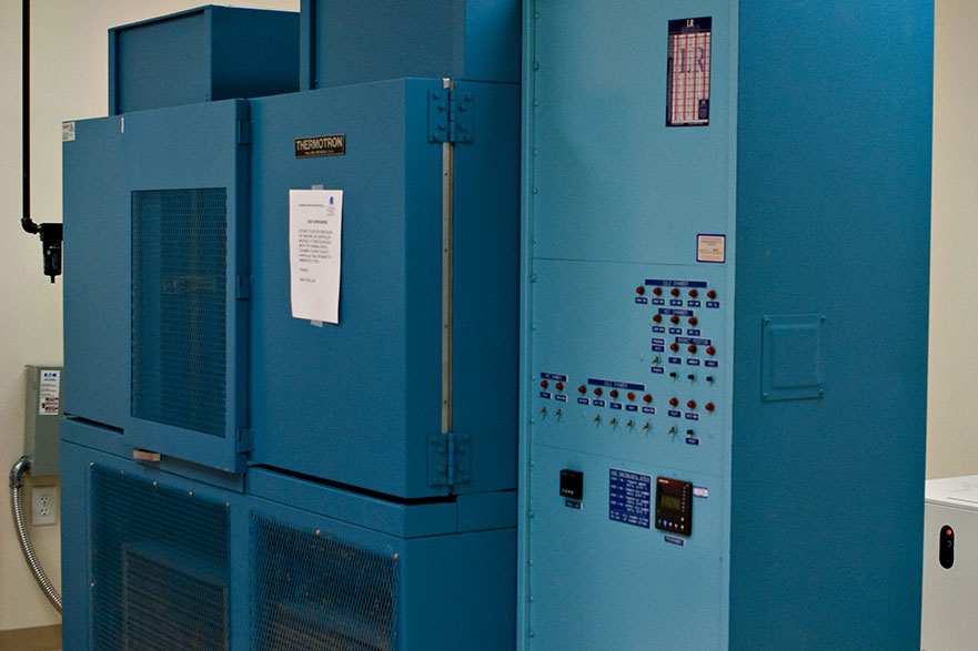
All electronic hardware is susceptible to the damaging effects of moisture, temperature, and contaminants. STI understands the criticality of reliability testing and test-to-failure. Improper selection of assembly materials and manufacturing processes can result in field failure returns which can lead to high warranty reserves thus affecting long-term profitability. STI offers an assortment of temperature/humidity test chambers, in addition to in-situ electrical testing capability, with which to perform testing per your specified requirements.
• Thermal Shock
• Temperature Cycling
• Moisture Resistance
• Humidity Cycling
• Shelf Life
• Accelerated Aging
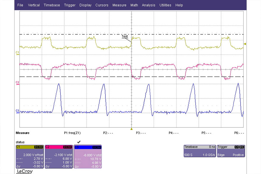
STI offers a variety of electrical test services from component-level testing/characterization to system-level testing. Electrical testing is offered to validate values in accordance with component manufacturer’s performance specifications, a customer’s test specification, as well as standard test methods.
• Component-Level Testing
• Passive Parametric Testing
• Discrete Failure Simulation
• IC Voltage/Current Analysis
• System-Level Testing
• Troubleshooting/Debugging
• Failure Analysis
• Insulation Resistance Testing
• IPC-TM-650
• HIPOT Testing (up to 1000 V)
• Cable Assemblies
• Printed Circuit Boards
• Circuit Card Assemblies
• Data Acquisition
• Voltage Monitoring
• Temperature Monitoring
STI offers an assortment of mechanical test services to characterize assembly materials and evaluate manufacturing process parameters. Mechanical testing capabilities include first-level interconnects, such as bond wire pull testing and die shear, in addition to second-level interconnects, such as SMD shear strength and solder bump shear strength for BGAs, CSPs, and WSPs.
• Bond Strength (Destructive)
• Nondestructive Bond Pull
• Die Shear Strength
• Solder Bump Shear Strength
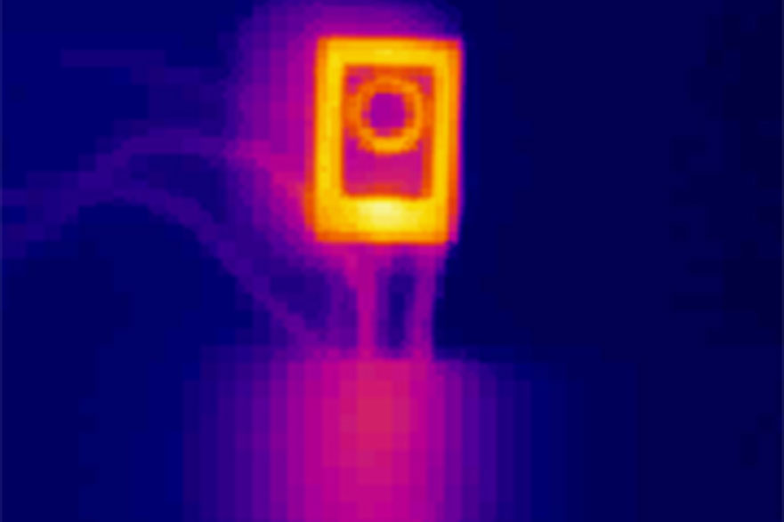
Thermal infrared (IR) imaging analysis aids dramatically in characterizing an electronics assembly’s thermal dissipation and identifying peak junction temperatures of the populated component set. The results from IR Thermography testing can influence printed wiring assembly design and thermal interface material selection to ensure low component junction temperatures and/or adequate assembly-level thermal dissipation. Conversely, IR Thermography testing may be used to identify a troublesome component or circuit within an assembly on either a lab workbench or as deployed in the field.
• Assembly Thermal Profiling
• Component Tj Analysis
• Electronics Failure Analysis

Strain gage testing is utilized to evaluate materials and processes effect on PWB and component-level stress due to static and dynamic loads. These stresses can originate from sources such as thermal, mechanical, and/or a combination of the two. STI offers strain gage testing and analysis services to characterize these stresses as a result of design, assembly materials, and/or assembly and test processes. If not addressed, these stresses can lead to microfractures and ultimately field returns due to failure. Identification and elimination of these stresses can greatly improve assembly yield and long term reliability of your electronics assembly.
• Strain Gage Rosette Selection
• Rosette Attachment and Wiring
• Data Acquisition with Thermal Correlation
• Stress/Strain Analysis
Analytical Lab
- Material Failure Analysis
- Qualification Testing
- Visual Inspection / IPC Compliance
- SEM / EDS
- Ion Chromatography
- Transmission X-Ray Evaluation
- Micro-Sectional Analysis
- XRF – Plating Thickness Evaluation
- Wetting Balance Testing
- FTIR – Organic Contamination Testing
- Dye & Pry Testing
- Supply Chain Validation
The experience and knowledge of STI’s Analytical Laboratory personnel enables interpretation of test results and reporting that lets our customers make the right choices for corrective actions. Services include Qualification testing, Visual Inspection & IPC Compliance Testing, residue/cleanliness analysis, and solderability testing. STI’s enhanced capabilities are the result of the recent addition of several new analytical tools and equipment. The analytical equipment includes some of the industry’s newest and most advanced tools. STI also provides services as an expert witness and arbitrator.
Qualification testing can be performed on bare boards (PCB) as well as electronic assemblies (PCBA). Testing on bare boards would be performed to ensure incoming bare board quality and conformance to any build specifications (e.g. IPC-A-600, IPC-6012 or customer specific test criteria). Such an investigation could include (but is not limited to) the following analytical methods:
• Visual Inspection
• Plating Surface Evaluation (SEM/EDS)
• Plating Thickness Evaluation (XRF)
• Plating Adhesion Testing
• Ionic Cleanliness Testing (IC)
• X-Ray Inspection
• SIR Testing
• Environmental Testing
• Micro-Sectional SEM Evaluation
These analytical methods would provide information on overall fabrication, plating adhesion quality and thickness, conductor and laminate dimensions, conductor solderability and through-hole integrity. Testing on electronic assemblies would be performed to ensure overall process quality and conformance to any built specifications (e.g. IPC-A-610, J-STD-001 or customer specific test criteria). Such an investigation could include (but is not limited to) the following analytical methods:
• Visual Inspection
• Surface Evaluation (SEM/EDS)
• X-Ray Inspection
• Ionic Cleanliness Testing (IC)
• Environmental Testing
• Micro-Sectional SEM Evaluation
These analytical methods would provide information on specification compliance, assembly cleanliness, overall solder joint integrity and long-term reliability of the hardware.
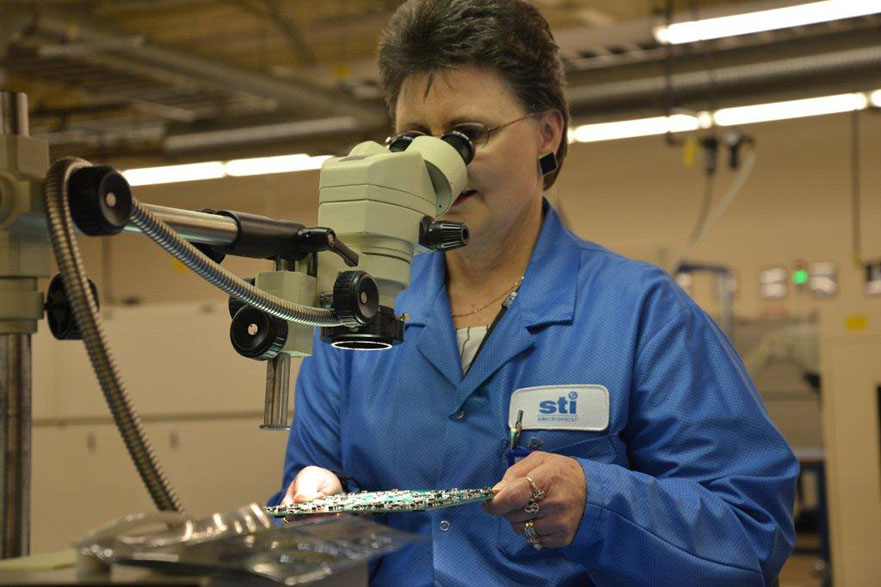
Visual Inspection / IPC-Compliance testing can be performed on bare boards (PCB) as well as electronic assemblies (PCBA). Such an investigation on bare boards (PCB) would consist of the visual interpretation of conformance / compliance to minimum requirements set forth in various printed board specifications, e.g; customer specific criteria, IPC-A-600 and IPC-A-610. Such an investigation on assemblies (PCBA) would consist of the visual interpretation of conformance / compliance to minimum requirements set forth in various electronic assemblies specifications, e.g; customer specific criteria or IPC-A-600 and IPC-A-610.

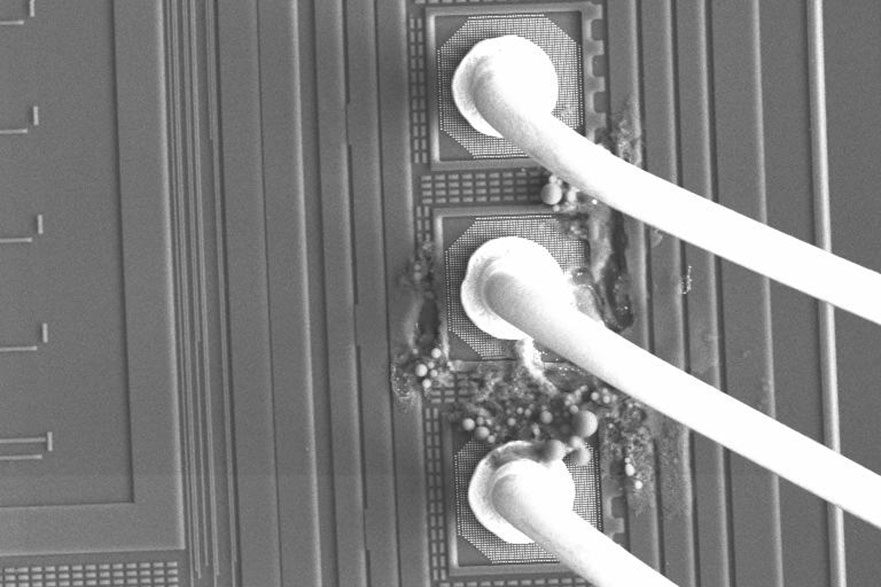
Scanning Electron Microscopy (SEM) is ideal for inspection of PCBAs, bare PCBs, electronic components or any other materials used in the industry. It enables visual inspection and both linear and geometric dimensional measurement at very high magnifications. This equipment has the capability of providing digital imaging of specimens with a magnification in the thousands, or simple exploratory analysis at low magnification for gross failure analysis and identification. Along with very high magnification capability from that of a traditional optical microscope is the very high depth of field, which allows for very detailed and easily interpretable images. This aids in the process of root cause failure analysis and subsequent reporting of failures. Finally the oversized specimen chamber allows for large samples on the order of 6” x 6” to be analyzed without destructive sample preparation,important for expensive hardware.
Secondary Electron imaging allows for surface topography mapping. Applications include fracture surface analysis, integrated circuit surface mapping, Micro Electro-Mechanical (MEM’s) inspection and analysis, surface residue analysis and external plating analysis. Backscattered Electron imaging allows for atomic number contrasting and imaging. Applications include contamination analysis, elemental phase mapping and identification and surface quality evaluations.
Energy Dispersive Spectroscopy (EDS) allows for characteristic x-rays emitted from a sample to be identified, allowing qualitative and quantitative elemental identification on a microscopic scale. In addition, elemental “mapping” can be utilized to produce an image detailing both the composition and structure of the different phases of materials present. Used in conjuction with SEM imaging, elemental identification provides a very powerful tool in evaluating manufacturing processes, materials selection, residue and corrosion identification and quantification, as well as other failure analysis efforts.
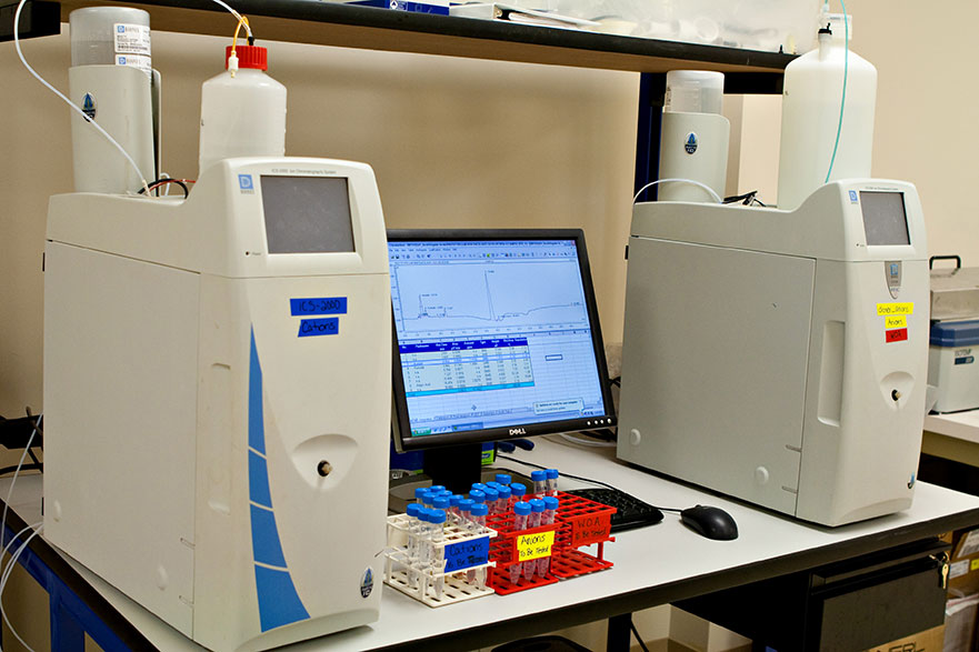
Ion Chromatography (IC) or Ionic Cleanliness testing is performed in compliance with IPC-TM-650, Method 2.3.28, “Ionic Analysis of Circuit Boards, Ion Chromatography Method”, on either bare boards (PCB) or electronic assemblies (PCBA). A conductivity detector measures the ionic activity, separated in anions, cations and weak organic acids, of the solvent extract from each individual sample presented in μg/in2.
Along with subject matter experts in the field of cleanliness and cleanliness testing, we offer real world experience and consultation for all your manufacturing cleanliness problems.
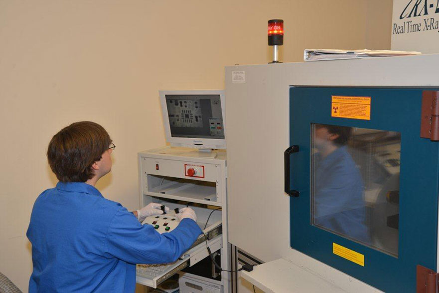
Real time transmission x-ray analysis allows for immediate non-destructive imaging of specimens. The extra large chamber permits specimens ranging from small micro ball grid arrays (BGA) to large circuit board assemblies (18” x 21”). Interior defect characterization is possible using the digitally projected x-ray image. As with the Scanning Electron Microscope (SEM), high-resolution images can be digitally captured or photo quality images can be printed depending on the requirements of the analysis. X-Ray inspection can be utilized for examination of the following examples:
• Ball Collapse in Ball Grid Arrays (BGA)
• Obvious Open Solder Connections
• Void Inspection
• Solder Bridges Between Adjacent Conductors
• Gold Wire-Bond Evaluation
• Through-Hole Barrel Fractures
• Internal Annular Ring Registration
• PCB Trace Inspection
Magnification up to 125 times can be accomplished allowing for inspection of features on the scale of individual wire bonds and flip chip ball interfaces.

Full micro-sectioning and sample preparation services are performed on-site for expediting failure analysis efforts. Once a failure site is located, micro-sectioning is performed and the subsequent analysis will identify the exact failure mechanism and root cause.

X-Ray Fluorescence Spectroscopy (XRF) allows for accurate quality control of printed circuit boards and electronics, by measuring plating thickness non-destructively. It can measure the plating thickness on large and fine-pitch conductors of a variety of plating finishes: tin-lead (Sn-Pb), immersion silver (ImAg), immersion tin (ImSn), electroless nickel immersion gold (ENIG) and thick gold (Au).
The solderability of a surface is defined by its solder wetting characteristics. Solder wetting pertains to the formation of a relatively uniform, smooth, and unbroken film of solder that exhibits excellent adherence on the soldered surface. Non-wetting, on the other hand, is the condition wherein the solder coating has contacted the surface but did not adhere completely to it, causing the surface or a part thereof to be exposed. Dewetting is the condition wherein the solder recedes after coating a surface, creating irregular mounds of solder, but leaving behind no exposed areas.
Wetting balance testing is a quantitative solderability test that measures the wetting forces between molten solder and the test surface as a function of time. The plot starts with the wetting force being negative (non-wet condition), which rises until it crosses the zero axis of wetting force, indicating that wetting has occurred. The time it takes for wetting to occur is one parameter used to assess solderability. It is utilized to measure the willingness to take solder on both leaded and non-leaded surface mount (SMT) and thru-hole (PTH) components, with either leaded or lead-free solder. Testing is performed per IPC J-STD-002, IPC J-STD-003 or Mil-Std-883 specifications.
Fourier Transform InfraRed Spectroscopy (FTIR) is most useful for identifying chemicals that are either organic or inorganic in nature. It relies on the identification of the types of chemical bonds (functional groups). The wavelength of light absorbed is characteristic of the chemical bond. FTIR spectra of pure compounds are generally so unique that they are like a molecular “fingerprint”. It can be utilized to quantitate some components of an unknown mixture. It can be applied to identify chemicals (e.g., fluxes, cleaners, coatings and contaminants). The spectrum of an unknown can be identified by comparison to STI’s library of known materials used within the industry.
The dye and pry technique relies on the ability of a very low viscosity dye to penetrate a fracture while under a high vacuum. Generally a vacuum is applied for several hours, followed by a high temperature bake to cure the dye. Next, the BGA component or QFN is mechanically removed and the interfaces inspected for any traces of the dye on the surface of the pads. If the bonds are intact, dye will not penetrate and stain the pads. However, if there is a complete or partial fracture, the dye will coat the fractured surface and subsequent inspection will identify the fractured solder joints.
STI Electronics is facilitated with the equipment set and personnel to complete a variety of tests and analysis on electronic assemblies as well as electromechanical assemblies to determine the integrity of the supply chain. Our methods can determine the origin of the components and materials in order to to identify counterfeit components and/or those which have been altered. We also work closely with software and firmware partners to identify and resolve malicious intent at the system level. From operating in a detection mode to identify gaps to developing a trusted supply chain, STI can also establish a project plan that will include a phased approach that is designed to optimize defining lessons learned which can be shared with the broader Trusted Systems and Networks community (DoD and Commercial). Our team composition is designed to include representatives from each stakeholder in the acquisition process. Phase I – defines the prototype scenario, developing an overall requirements specification and documenting the project plan to include deliverables. Phase II –implements the prototype project plan, mitigates the design manufacturing and packaging risks, and captures the lessons learned to repeat this process on a wider scale. Phase III – expands the prototype to other areas within these commercial and government communities to create a model for compliance for the supply chain associated with electronics and electromechanical assemblies at the hardware and system (software and firmware) level.
Microelectronics Cleanroom
- Microelectronics Packaging
- Microelectronics Assembly
- Imbedded Die Engineering (IC/DT®)
- Ultrasonic / Thermostatic Wire Bond
- Flip Chip Assembly
- Thermal Optimization
- Cleanroom (Class 1000 / ISO Class 6)
The Microelectronics Packaging Lab was established to meet the rising need for advanced systems development and packaging to address the emerging challenges and issues facing today’s electronics assemblies. Advanced design and modeling software enables STI to design and develop highly integrated hardware to meet shrinking form and fit factor requirements as well as increasing thermal loads. Emerging packaging materials are continuously evaluated to optimize electrical and thermal performance.
The microelectronics lab specializes in state-of-the-art packaging design and microelectronics assembly including current technologies such as Chip-On-Board (COB) and Multichip Module (MCM) as well as emerging technologies such as STI’s patented packaging technology termed Imbedded Component/Die Technology (IC/DT®).
STI’s involvement in research and development programs, both in component packaging technologies and electronics assembly manufacturing, has brought about the installation of the latest and most advanced equipment and the acquisition of the top people in this field. STI is staffed to design, develop, assemble, and test a ruggedized electronics assembly in an advanced cleanroom laboratory (Class 1000/ISO Class 6 certified) to meet our customer’s specifications.
A Class 1000 / ISO Class 6 cleanroom provides the optimum environment for prototype and low volume microelectronics manufacturing and assembly production.
Assembly materials such as printed circuit boards (PCBs), components, and wire are stored in dry nitrogen cabinets to reduce contamination and degradation.
A sophisticated dispenser/placement machine is used for low volume dispense accuracy and repeatability in addition to ±10 μm component placement. Component pick options include waffle pack and wafer for high-precision SMT and bare die, including flip chip assembly.
Wire bond interconnect is accomplished with a fully automatic ultrasonic wedge bonder utilizing aluminum wire over a wide diameter range for low and high current applications.
A two-channel mass flow controller plasma system is employed to prepare surfaces for die attach, wire bonding, and encapsulation.
Material qualification and process control are accomplished via a bond tester coupled with high magnification visual inspection.

• Semiconductor Packaging
• Chip & Wire Technology
• Flip Chip Attachment
• Mixed Assembly Technology
• Multichip Modules (MCM)
• Package-on-Package (PoP)
• System-in-Package (SiP)
• Materials Qualification
• ISO 9001:2008 Certified
• Smallest Form and Fit Factor
• Low Stress Interconnect Attach
• Passive Thermal Management
• Stress Compliant Materials
• Reduced Failure Opportunity
• Aluminum Ultrasonic Wedge Bonding
• Gold Thermosonic Ball Bonding
• Ribbon Bonding
• Direct Chip Attach (DCA)
• Lead-Free Interconnect
• Eutectic 63Sn37Pb Interconnect
• High Lead Interconnect
• Anisotropic Conductive Adhesive Interconnect
• Underfill Encapsulation

• Passive Cooling Design
• Thermal Material Selection
• Thermography Testing

An Class 1000/ISO Class 6 cleanroom provides the optimum environment for for prototype and low volume microelectronics manufacturing and assembly production. Assembly materials such as printed circuit boards (PCBs), components, and wire are stored in dry nitrogen cabinets to reduce contamination and degradation. A sophisticated dispenser/placement machine is used for low volume dispense accuracy and repeatability in addition to ±10μm component placement. Component pick options include waffle pack and wafer for high-precision SMT and bare die, including flip chip assembly. Wire bond interconnect is accomplished with a fully automatic ultrasonic wedge bonder utilizing aluminum wire over a wide diameter range for low and high current applications. A two-channel mass flow controller plasma system is employed to prepare surfaces for die attach, wire bonding, and encapsulation. Material qualification and process control are accomplished via a bond tester coupled with high magnification visual inspection.
• ISO 14644-1 Certification to ISO Class 6
• Controlled Temperature/Humidity Environment
• Ionizer/Dissipative Flooring ESD Control
Request a quote
Please fill the form below for any Manufacturing, Engineering, Analytical Lab or Cleanroom requests!


